
Semiconductor Bonding Market Analysis Report 2023-2032:
- Report ID: ME_00132326
- Format: Electronic (PDF)
- Publish Type: Publish
- Number of Pages: 250
Market Snapshot
Source: Market Expertz

| Study Period | 2019-2032 |
| Base Year | 2023 |
| Forcast Year | 2023-2032 |
| CAGR | 9.14 |


Gain accurate insights regarding the negative impacts of COVID-19 on all markets and industries
Download Sample PdfReport Overview
The Semiconductor Bonding Market is projected to grow with a Compound Annual Growth Rate (CAGR) of 5.87% between 2022 and 2032. The market size is expected to expand by USD 13,784.21 million during this period. The market's growth is influenced by various factors, including the increasing demand for miniaturized and high-performance electronic devices, the emergence of advanced packaging technologies, and the rise in demand for advanced semiconductor materials. Semiconductor bonding refers to the process of joining two or more semiconductor wafers or chips together to create integrated structures, enabling enhanced performance and functionality in electronic devices. This technique involves various methods like die-to-die bonding, chip-to-wafer bonding, and wafer-level packaging, aimed at achieving greater compactness and efficiency in electronic components.
Semiconductor Bonding Market Overview:
Drivers:
The demand for miniaturized and high-performance electronic devices is a significant driver of the semiconductor bonding market. As electronic devices continue to become smaller and more powerful, the need for innovative packaging and bonding techniques has intensified. Semiconductor bonding enables the integration of multiple chips or components in a compact manner, enhancing device performance and reducing the overall footprint.
Additionally, the adoption of advanced packaging technologies, such as 3D IC packaging and system-in-package (SiP), is driving the growth of the semiconductor bonding market. These packaging techniques offer higher interconnect densities and improved electrical performance, leading to increased demand for advanced bonding solutions.
Trends:
The integration of advanced materials in semiconductor bonding is a prominent trend in the market. The use of materials like copper, low-k dielectrics, and new substrate materials enables higher performance, improved thermal management, and greater reliability in bonded semiconductor structures. This trend is particularly important as devices become more sophisticated and demanding in terms of thermal and electrical properties.
Furthermore, the development of wafer-level packaging (WLP) and fan-out wafer-level packaging (FO-WLP) techniques is shaping the semiconductor bonding market's growth. WLP and FO-WLP allow for the integration of multiple chips onto a single wafer, reducing costs, enhancing performance, and enabling the creation of more compact electronic devices.
Restraints:
Technical challenges and manufacturing complexities represent significant restraints for the semiconductor bonding market. Achieving precise alignment and uniformity during the bonding process requires advanced equipment and specialized expertise, leading to higher production costs and potential yield issues. Additionally, the adoption of novel bonding methods may require modifications to existing manufacturing processes, leading to potential disruptions in the supply chain.
Moreover, the integration of advanced materials and techniques may lead to compatibility issues, as the characteristics of different materials and processes need to align seamlessly for successful bonding. This challenge can result in lower yields and increased costs during the initial stages of implementation.
Semiconductor Bonding Market Segmentation by Application:
The consumer electronics segment is anticipated to witness substantial growth during the forecast period. Semiconductor bonding plays a critical role in enhancing the performance and functionality of consumer electronic devices such as smartphones, tablets, and wearables. As consumer expectations for faster processing speeds, higher-resolution displays, and longer battery life continue to rise, semiconductor bonding enables the integration of diverse components, such as processors, memory, and sensors, in a compact and efficient manner.
Semiconductor Bonding Market Segmentation by Type:
The 3D IC bonding segment is experiencing robust growth driven by the increasing adoption of three-dimensional integrated circuits in various applications. 3D IC bonding enables the stacking of multiple semiconductor dies, leading to enhanced performance and reduced interconnect lengths. This type of bonding is particularly valuable for high-performance computing, data centers, and advanced mobile devices.
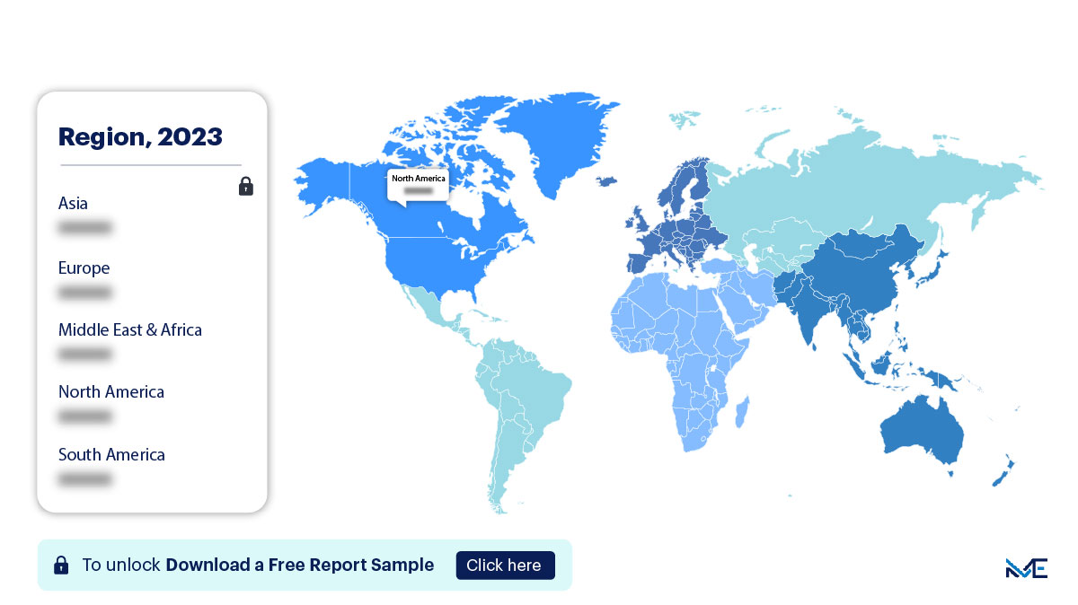
Regional Overview:
Download the report summary now!
Request pdf Sample
The Asia-Pacific (APAC) region is projected to contribute significantly, accounting for 50% of the global semiconductor bonding market's growth during the forecast period. APAC's dominance is attributed to its status as a hub for semiconductor manufacturing, with countries like China, Taiwan, and South Korea hosting major semiconductor foundries and packaging facilities. The presence of leading players in the semiconductor ecosystem and substantial investments in research and development further amplify the region's influence on the market.
The impact of the COVID-19 pandemic on the semiconductor bonding market varied across regions. While the initial phases of the pandemic led to disruptions in supply chains and manufacturing operations, the gradual recovery and adaptation of the industry contributed to the market's resilience. As vaccination efforts gained momentum, the semiconductor ecosystem regained stability and saw renewed growth.
Semiconductor Bonding Market Customer Landscape:
The semiconductor bonding market's customer landscape encompasses a wide range of industries, from consumer electronics and automotive to healthcare and aerospace. The adoption of semiconductor bonding technologies varies across industries based on factors such as performance requirements, cost constraints, and technological advancements. Companies in different stages of adoption, from early innovators to mainstream adopters, shape the market dynamics.
Major Semiconductor Bonding Market Companies:
Companies in the semiconductor bonding market employ diverse strategies, including collaborations, acquisitions, and product launches, to expand their market presence and meet evolving customer needs.
- Amkor Technology Inc.
- ASM Pacific Technology Ltd.
- Besi Group
- EV Group (EVG)
- Kulicke & Soffa Industries Inc.
- Palomar Technologies Inc.
- SHINKAWA Ltd.
- SUSS MicroTec SE
- Tokyo Electron Limited (TEL)
- Toray Engineering Co. Ltd.
The competitive landscape of the semiconductor bonding market is marked by strategic partnerships, technological innovations, and a focus on expanding product portfolios to cater to diverse applications and industry requirements.
Segment Overview:
The semiconductor bonding market report provides revenue forecasts at global, regional, and country levels, analyzing trends and growth opportunities from 2019 to 2032.
- Application Outlook (USD Million, 2019 - 2032):
- Consumer Electronics
- Automotive
- Healthcare
- Industrial
- Others
- Type Outlook (USD Million, 2019 - 2032):
- Die-to-Die Bonding
- Chip-to-Wafer Bonding
- Wafer-Level Packaging (WLP)
- Others
- Geography Outlook (USD Million, 2019 - 2032):
- North America
- The U.S.
- Canada
- Europe
- U.K.
- Germany
- France
- Rest of Europe
- APAC
- China
- Japan
- South Korea
- Rest of APAC
- South America
- Brazil
- Argentina
- Rest of South America
- Middle East & Africa
- UAE
- South Africa
- Rest of Middle East & Africa
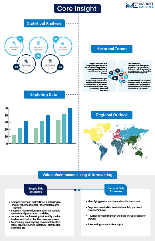
RESEARCH METHODOLOGY
A research methodology is a systematic approach for assessing or conducting a market study. Researchers tend to draw on a variety of both qualitative and quantitative study methods, inclusive of investigations, survey, secondary data and market observation.
Such plans can focus on classifying the products offered by leading market players or simply use statistical models to interpret observations or test hypotheses. While some methods aim for a detailed description of the factors behind an observation, others present the context of the current market scenario.
Now let’s take a closer look at the research methods here.
Secondary Research Model
Extensive data is obtained and cumulated on a substantial basis during the inception phase of the research process. The data accumulated is consistently filtered through validation from the in-house database, paid sources as well reputable industry magazines. A robust research study requires an understanding of the overall value chain. Annual reports and financials of industry players are studied thoroughly to have a comprehensive idea of the market taxonomy.
Primary Insights
Post conglomeration of the data obtained through secondary research; a validation process is initiated to verify the numbers or figures. This process is usually performed by having a detailed discussion with the industry experts.
However, we do not restrict our primary interviews only to the industry leaders. Our team covers the entire value chain while verifying the data. A significant number of raw material suppliers, local manufacturers, distributors, and stakeholders are interviewed to make our findings authentic. The current trends which include the drivers, restraints, and opportunities are also derived through the primary research process.
Market Estimation
The market estimation is conducted by analyzing the data collected through both secondary and primary research. This process involves market breakdown, bottom-up and top- down approach.
Moreover, while forecasting the market a comprehensive statistical time series model is designed for each market. Macroeconomic indicators are considered to understand the current trends of the market. Each data point is verified by the process of data triangulation method to arrive at the final market estimates.
Final Presentation
The penultimate process results in a holistic research report. The study equips key industry players to undertake significant strategic decisions through the findings. The report encompasses detailed market information. Graphical representations of the current market trends are also made available in order to make the study highly comprehensible for the reader.
Personalized Business Report Tailored to Your Requirements
- Our expert analysts collaborate directly with you to comprehend your specific needs.
- Get data on regions, segments, competitors, and vendors of your choice.
- Information is presented in alignment with your exact preferences and formatting.
Free Sample Report
"Find new revenue generation opportunities"